Nanoengineering of Materials and Devices

Ural Federal University named after the First President of Russia B. N. Yeltsin
Подать документы
3
Contract-based places
13
places on a budget basis
373 000
Cost of tuition per year

About the training program

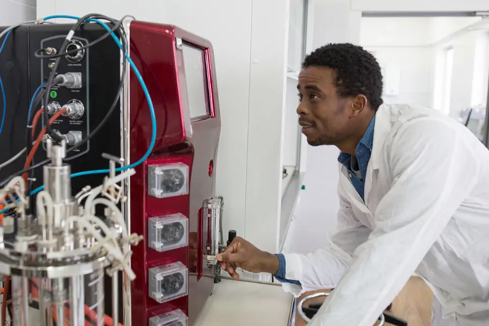
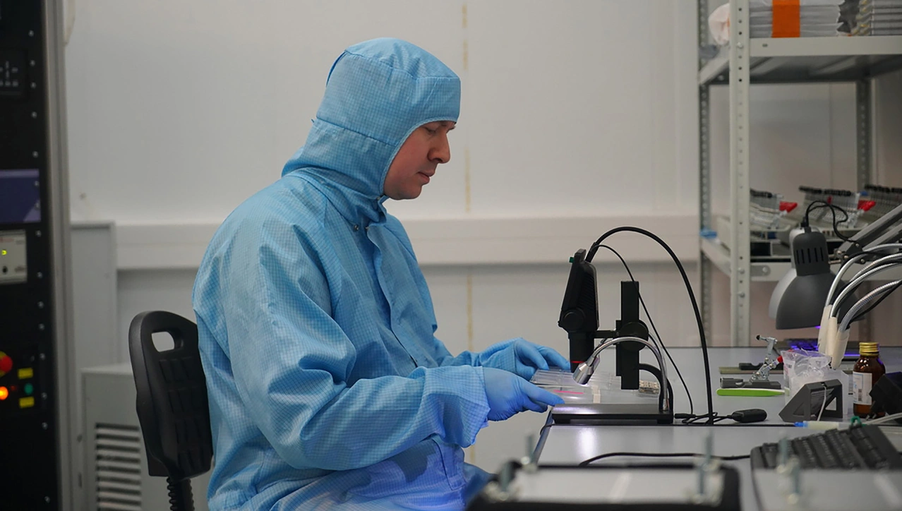
The programme is designed to train highly qualified specialists in nanoengineering who are able to solve professional tasks in a wide range of work situations. The programme covers nan particle production technologies, scanning probe microscopy methods, nanolithography, radiation technologies, and materials for organic electronics. Special attention is paid to the application of artificial intelligence in materials science. Students master numerical modelling of nanostructure properties and work with unique equipment in the laboratories of the Institute of Metallurgy of the Ural Branch of the Russian Academy of Sciences; some of the facilities have no equivalents anywhere in the world.

What will they teach you?

  • Методам численных расчетов и моделирования свойств наноматериалов и нанообъектов
  • Методам зондовой микроскопии и нанолитографии
  • Технологии получения новых наноматериалов, способных работать в экстремальных условиях
  • Современным методам получения наночастиц и упорядоченных наноструктур
  • Применению прикладного программного обеспечения и освоению основных технических средств численных расчетов

What do graduates do?

The program trains specialists in the physics of nanomaterials and nanostructures to work in laboratories at research institutes, in enterprises developing and manufacturing high-tech products, as well as researchers and teaching staff working at higher education institutions.

Pass score on budget

2026
74
2025
67
2024
71

Entrance exams

Exam 1 of 1

Interview

Our other training programs

Hello!Shall we talk?Ask questions!I will answer any question!Any questions?Ask!Any questions left?Ready to help!I will be glad to help!Click on me!